ZEISS Events

ZEISSテクニカルカンファレンス2024

最先端研究イノベーターによるZEISS顕微鏡技術のご紹介

最先端研究に取組まれているイノベーターの方々に、ZEISS Xradia Versa, GeminiSEM, Crossbeamを活用した最新事例をご紹介いただきます。
ZEISS製品をお使いいただいている方はもちろん、今までご利用経験の無い方もご自身の研究の参考となる貴重なお話を聴いていただける機会です。是非ご参加ください。

ZEISSテクニカルカンファレンス2024 

最先端研究イノベーターによるZEISS顕微鏡技術のご紹介

日時

2024年5月24日(金)
10:00 – 17:40(9:30受付開始)/ 懇親会 18:00 ~  ※予定

会場

東京ミッドタウン八重洲カンファレンス 4階
セミナー 大会議場2
懇親会 大会議場1

東京都中央区八重洲 2-2-1 東京ミッドタウン八重洲セントラルタワー MAP

アクセス

JR「東京」駅 地下直結(八重洲地下街経由)、東京メトロ丸の内線「東京」駅 地下直結(八重洲地下街経由)
東京メトロ銀座線「京橋」駅 徒歩3分
東京メトロ東西線、銀座線、都営浅草線「日本橋」駅 徒歩6分

定員・締切

100名限定
セミナー・懇親会の参加は無料です。※昼食付 
定員になり次第、受付を終了いたします。

参加方法

参加登録フォームよりご登録ください。

注意事項

  • お問合せ・ご質問は こちら までご連絡をお願いいたします。
  • 同業他社の方のお申し込みはご遠慮ください。
  • 本セミナーの録画は公開いたしません。
  • 講演者の記載は順不同です。
  • 本ページで紹介する講演者の記載順は、登壇順や役職などを表すものではありません。 あらかじめご了承ください。
基調講演

トポロジカルスピン構造とその駆動ダイナミックスの実空間観察

国立研究開発法人理化学研究所
創発物性科学研究センター
電子状態マイクロスコピー研究チームリーダー
于 秀珍

スキルミオンは、極めて低い電流密度で駆動可能であり、省エネルギーデバイスやリザバーコンピューティング素子などへの応用が期待されています。私たちは、スキルミオンの存在が可変磁場下のローレンツ電顕法で、世界で初めて実証されました。また、ある厚みの試料において、スキルミオン紐の存在も予想され、位相トモグラフィーを用いてスキルミオン紐の存在が明らかになりました。本講演では、様々な磁性体中で励起されたスキルミオンを含むさまざまなスピン構造とその電流駆動ダイナミクスをご紹介いただきます。

FIB/ULV-SEM複合機を用いた燃料電池材料の三次元構造解析

JFEテクノリサーチ株式会社
機能材料ソリューション本部
ナノ解析センター(千葉駐在)
主査
池本 祥

固体高分子形燃料電池材料(MPL、セパレータ)などを題材に、Crossbeam 540を用いた解析事例を複数ご紹介いただきます。Geminiカラムを有する極低加速電圧SEMとしての表面・断面観察活用事例、およびFIB-SEM複合機として用いた三次元構造解析事例をご紹介。後者の事例では、数nmピッチのFIB加工と加速電圧:1kV未満でのSEM観察を組み合わせることで、ナノメートルオーダーの空隙率解析が可能なことをお話いただきます。

キーポイント
・FIB-SEM複合機による三次再構築
・極低加速電圧SEM観察
・燃料電池

GeminiSEM 560を用いたトナーの観察事例紹介

キヤノン株式会社 
周辺機器事業本部 化成開発センター 
化成第二開発部 化成24開発室
田村 繁人

電子写真装置で粉体インクとして用いられるトナーは帯電しやすく、さらにトナー表面は多種の外添剤で被覆されています。
①トナー表面の高倍率観察に課題があり、そこで低加速電圧に特化した最新GeminiSEMの特長を活かした観察事例をご紹介いただきます。
②トナーは複数の樹脂で構成され、それらを区別した可視化に課題があります。そこで樹脂材料別染まりやすさの違いを利用した染色技術を前処理として用いた観察事例についてもご紹介いただきます。

キーポイント
・帯電しやすい試料
・微粒子の観察
・樹脂材料を区別した可視化(染色技術)
・低加速電圧反射電子像観察

Analysis of crystal defects by electron channelling contrast imaging (ECCI) for the advancement of structural materials.

Max Planck Institute
Group Leader
Department Microstructure Physics and Alloy Design
Microscopy and Diffraction
Dr. Stefan Zaefferer

Electron channelling contrast imaging (ECCI) is an SEM based technique for observation of extended crystal lattice defects like dislocations and stacking faults. It exploits the dependence of the backscatter electron intensity on crystal orientation and atomic order. For ECCI a crystalline sample is observed with the backscattered electron signal. The basic principle of contrast formation is that electrons channel into a crystal lattice when the incident beam hits the lattice along the Bragg angle of a set of crystal planes. In this case, very few electrons are backscattered and the observed crystal appears dark. Every defect that disturbs the order of the lattice planes, in contrast, leads to backscattering and is visible in the ECC image as bright features in a dark grain. Dislocations, for example, appear as bright lines, stacking faults as bright areas.
The technique can be used very similar to transmission electron microscopy (TEM), however with the serious advantage that a bulk sample is observed and not a thin foil. This enables observation of much larger samples, simplifies sample preparation, and it facilitates in-situ experiments like deformation, heating, or gas reaction observations. Zeiss SEMs based on the Gemini column offer a number of advantages for ECCI, the most important being the high resolution at conditions where small beam convergence and high beam current prevail. Additionally, the highly sensitive backscatter detector and the versatile stage (at best 6-axis) facilitate the imaging.
In the presentation the basic principles of the technique are explained and illustrated. The power of the technique is illustrated with examples of observations on superalloys and high strength steels.

群馬大学が果たすべき多様な役割に応えるために選んだGeminiSEM 560

国立大学法人群馬大学 
研究・産学連携推進機構 
機器分析センター
林 史夫

国立大学法人には機器分析センターそれに類するセンターが設置されています。これらセンターの現代社会における役割は、設置大学の研究推進、近隣企業の研究・開発支援及び研究・開発人材のリスキリング、分析に対する考え方・スキルを身に着けた人材の輩出、そしてそれらを具現化できる設備の選定・整備戦略など多岐にわたり、共用設備をマネジメントするセンターの重要性が増してきています。このような背景の中、GeminiSEM 560を選んだ理由、分析事例をご紹介いただきます。

キーポイント
・機器分析
・産学連携
・電界放出型走査電子顕微鏡
・GeminiSEM
・ナノテクノロジー
・群馬大

Katana ブロックフェースイメージングのご紹介 ~超音波ダイヤモンドナイフ切削によるVolume EMデータ構築~

メイワフォーシス株式会社
矢代 将栄

ご使用されているSEMを利用してSBF-SEM観察を実現する“Katana”をご紹介いただきます。KatanaはSEM試料室内で超音波ダイヤモンドナイフを用いたウルトラミクロトームにより切削を行い、その断面をSEM観察したデータから3D SEM像を構築することが可能になります。本講演では、Katanaの特長、生体試料やリチウムイオン電池正極材などのアプリケーション事例の紹介、GeminiSEMをはじめとしたFE-SEMへの搭載事例についてご紹介いただきます。

キーポイント
・Katana
・SBF-SEM
・Volume EM

Materials ScienceにおけるAIを用いた次世代高度3D画像解析技術 ~X線顕微鏡/電子顕微鏡用Dragonfly 3D World with Deep Learning~

株式会社マックスネット
上村 逸郎 

Easy to Use! 画像解析は優しさの次世代へ。Dragonfly 3D World with Deep Learningは、AI関連の豊富な機能と圧倒的なユーザービリティで、ユーザーの2D/3D/4D画像処理・解析のレベルを引き上げます。本セミナーでは、Dragonflyの主要な解析機能(2D/3D表示、ノイズ除去、繊維・粒子解析)とX線顕微鏡/電子顕微鏡での活用事例、AIセグメンテーション(Segmentation Wizard)の実際についてご紹介いただきます。

キーポイント
・3D解析
・Dragonfly
・Deep Learning
・セグメンテーション
・画像解析

Workflows and Capabilities enabled with Zeiss crossbeam laser

Carl Zeiss Microscopy GmbH, Germany
Product manager for Crossbeam laser and FESEM
Lamya Abdellaoui

The new technological improvement of all type of materials, including functional, semiconductors, micro-electro-mechanical, medical, needs a proper microstructure investigation from mm- up to nm-scale. One of the most used techniques is the focused ion beam (FIB), with a Ga+ beam for materials removal and specimen preparation for much high resolution techniques such as (TEM, APT ,..etc ). However, the material removal rate of FIB is very limited and time consuming for most applications. Hence, attaching a laser to cut faster into the FIB system is becoming a good strategy for rapid site-specific samples preparation at large scale [1].

Zeiss Crossbeam new generation combines a femtosecond laser source in a FIB/SEM for higher accuracy and resolution imaging to enables the fastest workflows. In addition, to this, contamination issues of the SEM/FIB chamber are considered, for this an isolated laser chamber is designed to prevent the contamination of electron column and detectors. At the meantime, the crossbeam system is well integrated by guaranteeing an easy and accurate sample transfer between the SEM and laser chamber under vacuum.

In this talk we will explore the capabilities and workflows enabled with the Zeiss crossbeam laser using a short, pulsed femtosecond laser <300 fs to cut > 1 mm3 of Si piece as an example in only 5 mins. The short pulses regime offers minimal to no artifacts from laser heat affected zone which reduces the thermal damaged happened with the laser and grant a better process control with less edges or curtaining. Thus, a direct visibility of the region of interest after laser preparation. Several examples will be shown providing the fastest time to results for cross-sectional analysis of deeply buried features at nanoscale resolutions.

Finally, new launched developments of the crossbeam laser will be presented
References:
[1] Manuel Pfeifenberger Desertation “ Implementation of femtosecond laser processing for materials testing and research “ Matriculation Number: 00831365, Erich Schmid Institute of Materials Science Austrian Academy of Sciences, Leoben.
Abstract based on marketing materials provided in Zeiss webpage

3D X-ray microscopy for advanced material characterization: how deep learning is pushing the limits of 3D imaging

カールツァイス株式会社
プロダクトアンドアプリケーション セールススペシャリスト
山本 千智
(Zeiss Research Microscopy Solutions, Dublin CA Hrishikesh Bale)

In the realm of advanced materials, novel applications often lead to the development of unique structures. Understanding the microstructure and its influence on material properties is crucial for designing and optimizing these materials. Metal Matrix Composites (MMCs) represent a class of materials with remarkable mechanical, thermal, and electrical properties. These composites consist of a metallic matrix reinforced with ceramic or other non-metallic phases. In this study, we delve into the comprehensive characterization of Ni-Ti-C-based MMCs fabricated using the laser engineered net shaping (LENS) process using X-ray microscopy. These advanced materials exhibit intricate microstructures that span a wide range of length scales, with various phases playing a critical role in determining their exceptional properties. Leveraging the high-resolution and non-destructive capabilities of X-ray microscopy, we gain invaluable insights into MMCs. By analyzing the microstructure at the sub-micron level, X-ray microscopy enables us to understand the spatial distribution and alignment of reinforcing phases within the metal matrix. Notably, some phases within the titanium carbide (TiC) domains push the limits of X-ray microscopy detection, relying on X-ray-to-visible-light conversion via scintillators coupled with optical magnification objectives. To overcome previous limitations, we employ a unique combination of specially designed high-resolution objectives and deep-learning-based 3D reconstruction. This approach yields sub-micron resolution results for dense and large MMC samples, which were previously impractical due to signal-to-noise constraints and the operating limits of X-ray scintillators. The integration of new-generation scintillator technology and the DeepScout technique enables this non-destructive feat. X-ray microscopy emerges as a powerful tool for materials characterization, offering high resolution and non-destructive capabilities, thus opening new avenues for optimized design and engineering.

大量データ取得を支援する高分解能SEMの自動化

カールツァイス株式会社
プロダクトアンドアプリケーション セールススペシャリスト
小田 武秀(会場)
風間 大和(デモルーム)
※LIVE配信(会場のみ)

近年では夜間大量データ取得やデータ駆動型研究のための走査電子顕微鏡(SEM)の無人化や夜間測定の需要が増し、高分解能SEMでも自動化のニーズが高まっています。今回、ZEISS Solutions Labで新たに開発したEM Toolkit「Visual workflow builder」のご紹介を弊社のデモルームから会場へ直接お届けいたします。このLIVE配信を通じて、ZEISS製品についてより深く理解していただけると幸いです。

ZEISS Microscopy Solutions

ZEISS GeminiSEM

極低加速フィールドエミッション走査型電子顕微鏡(FE-SEM)

ZEISS Sigma

汎用フィールドエミッション走査型電子顕微鏡(FE-SEM)

ZEISS Crossbeam

集束イオンビーム加工観察装置(FIB-SEM)
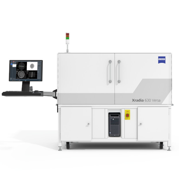
ZEISS Xradia Versa

3D X線顕微鏡(XRM)

参加登録フォーム

こちらのフォームから参加登録をお願いいたします。

フォームを読み込み中…